A Half Adder is the most basic digital arithmetic circuit. It performs the binary addition of two-bit binary numbers. One that performs the Binary Addition of 3-bit binary numbers is called the Full Adder.
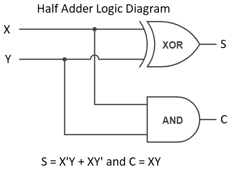
A Half Adder has two inputs and two outputs. The two input variables are called the Augend and the Addend bits and they are represented by X and Y in the circuit diagram. The output variables are the Sum and the Carry. And they are represented by S and C.
The sum output represents the least significant bit while the carry output represents the most significant bit of the binary addition.
Now the question arises here why does a Half Adder need two output variables?
The answer to this question is as: since the result of binary addition of two bits are 00, 01, and 10. The first two results, 00 and 01, need only one bit to represent them because the most significant bit in both is 0. But the last output 10 will need two bits to represent it because its most significant bit is 1.
Half Adder Circuit Diagram and Truth Table
The Half Adder circuit diagram is shown below. It consists of a XOR gate and an AND gate. The two-input XOR gate is used to produce the sum output while the two-input AND gate is used to generate the carry output of it.
The Half Adder truth table is given below. The Carry output of it will be 0 if both the inputs are 0 or one of them is 0. And it will be 1 if both the inputs are 1.
The Sum output of it will be 0 if both the inputs are either 0 or 1. And it will be 1 if one of the inputs is 0 and the other input is 1.
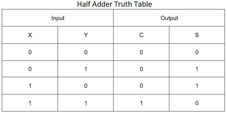
The Boolean equations for the two outputs can be obtained directly from the truth table.
S = X’Y + XY’, and
C = XY
NAND Gate using Half Adder
A NAND Gate can be implemented using Half Adders. We need two Half Adders to implement it. The circuit diagram of a NAND Gate using Half Adders is shown below.
Let HA1 and HA2 be two Half Adders. HA1 represents the first Half Adder while HA2 denotes the second Half Adder.
Let X and Y are the two inputs of HA1 and C be the carry output of it. The value of C will be XY because the carry output of a Half Adder is obtained from the AND Gate operation.
Now the carry output generated by HA1 will work as the first input for the HA2. We have to assign the second input of HA2 1 to get the Boolean Equation of a NAND gate
Now, let S be the sum output of the HA2. As we know that the sum output of a Half Adder is obtained from the XOR gate operation. Therefore we are going to apply the XOR gate operation on the two inputs of the HA2.
S = 1’XY + 1(XY)’
[Since 1’ = 0]
S = 0XY + (XY)’
S = 0 + (XY)’
S = (XY)’ Finally, the value of S is equivalent to the output of a two-input NAND Gate.

NOR Gate Using Half Adder
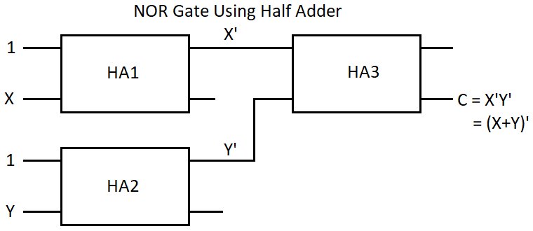
As we have implemented a two-input NAND gate using Half Adders. In the same manner, we can also implement a two-input NOR gate using Half Adders. To implement this gate we need 3 Half Adders. The Block Diagram of a NOR gate using Half Adders is shown below.
Let HA1, HA2, and HA3 be three Half Adders. HA1 and HA2 will be used to get the complement of inputs. The sum output of HA1 will give the complement of X when its inputs are X and 1. Similarly, the sum output of HA2 will generate the complement of Y when its inputs are Y and 1.
These two sum outputs of HA1 and HA2 will act as inputs for the HA3. The carry output of HA3 will give the output equation of a two-input NOR gate.
C = X’Y’
[By First De Morgan’s Theorem]
Or C = (X + Y)’
Finally, the Carry output of the third Half Adder is equivalent to the output of a two-input NOR Gate.
Half Adder Using Decoder
As we have created a Full adder using a decoder in our Full Adder topic, in the same way, we can also make a Half Adder using a decoder.
Now, the question arises here which decoder do we have to use to make a Half Adder?
The answer to this question lies in the diagram of the Half Adder. We know that a Half Adder has only two inputs. So we have to use a two-input decoder.
From the above Half Adder Truth Table, where X and Y are input to it and S and C are the output of it. We can write the Boolean functions for S and C.
S (X, Y) = ∑m (1, 2), and
C (X, Y) = ∑m (3)
Now, we use a 2-to-4 line decoder to implement the circuit diagram of a Half Adder. Since a decoder is a minterm generator, we can use those minterms to represent the Boolean function of S and C.
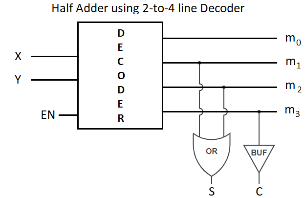
The above picture shows the circuit diagram of a Half Adder using a 2-to-4 line decoder, one OR gate, and one Buffer gate. Here X and Y are the inputs to the decoder. EN is the enable input that follows active high logic. It means that the decoder gets active when enable input is 1. m0, m1, m2, and m3 are the four minterms of the decoder.
We know that the sum output of a Half Adder is X’Y + XY’. To get this result we have to apply OR gate operation on m1 and m2 minterms of the Decoder. Thus we can write
S = m1 + m2
Or S = X’Y + XY’
Similarly, we know that the carry output of the Half Adder is XY. And this output can be obtained using a Buffer Gate on m3 minterm of the Decoder. Thus we can write
C = m3
Or C = XY
Half Adder Using Multiplexer
In the above topic, we have implemented a Half Adder circuit by using a decoder that generates the outputs of a Half Adder. In the same manner, we can implement it by using multiplexers too. We can design it by using 4 X 1 multiplexers and 2 X 1 multiplexers.
Half Adder Using 4 X 1 Multiplexer
Here, I am going to show you how we can design a Half Adder by using 4 X 1 Multiplexers. First of all, we need to write down the Boolean functions of sum and carry outputs as we have done above.
S (X, Y) = ∑m (1, 2) and,
C (X, Y) = ∑m (3)
Here, X and Y represent the two inputs and S and C represents the two outputs of the Half Adder.
Now the general output equation of a 4 X 1 multiplier is as follows:
Y = I0S’1S’0 + I1S’1S0 + I2S1S’0 + I3S1S0 ….. (1)
Where Y is the output, S1 and S0 are the selection inputs, and from I0 to I3 are the inputs of the 4 X 1 multiplexer.
The output equation of sum out of Half Adder is as follows:
S = ∑m (1, 2)
= m1 + m2
= X’Y + XY’
= 0.X’Y’ + 1.X’Y + 1.XY’ + 0.XY …… (2)
On comparing equation (1) and equation (2) we have, I0 = 0, I1 = 1, I2 = 1, I3 = 0, S1 = X, and S0 = Y.
The output equation of carry output of the Half Adder is as:
C = ∑m (3)
= m3
= XY
= 0.X’Y’ + 0.X’Y + 0.XY’ + 1.XY ….. (3)
On comparing equations (1) and (3) we get, I0 = 0, I1 = 0, I2 = 0, I3 = 1, S1 = X, S0 = Y.
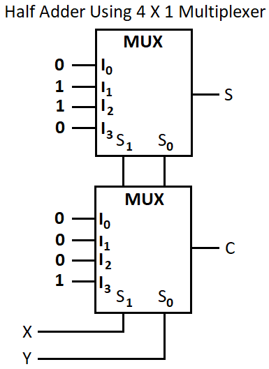
From the above picture, it can be stated that to implement the logic diagram of a Half Adder we need two multiplexers the first multiplexer produces sum output and the second MUX generates the carry output of the Half Adder.
X and Y are the two selection inputs to both multiplexers to select a particular input. The values of inputs of both multiplexers are obtained by comparing equations (1) and (2) and equations (1) and (3). This is the required logic diagram of a Half Adder using 4 X 1 multiplexers.
Half Adder Using 2 X 1 Multiplexer
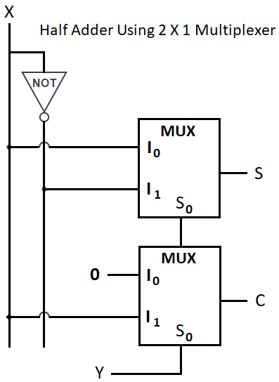
Here we will implement the logic diagram of a Half Adder using two 2 X 1 multiplexers. The first multiplexer will be used to find the S output while the second multiplexer will be used to generate the C output of Half Adder. The general output equation of a 2 X 1 multiplexer is as follows:
Y = I0S’0 + I1S0 ….. (1)
Where Y is the output, SO is the selection input line which selects a particular input at a time, and I0 and I1 are the inputs to the multiplexer.
Now the general output equation of sum output of a Half Adder is written as:
S = ∑m (1, 2)
= m2 + m1
= XY’ + X’Y …… (2)
On comparing equations (1) and (2) we have, I0 = X, I1 = X’ and S0 = Y.
Next the general output equation of carry output of Half Adder is as follows:
C = ∑m (3)
= m3
= XY
= 0XY’ + XY
= (0 × X)Y’ + XY
= 0Y’ + XY ….. (3)
On comparing equations (1) and (3) we have, I0 = 0, I1 = X and S0 = Y. The logic diagram of Half Adder using 2X1 multiplexers is given below.
