An AND Gate is an electrical circuit that embodies the logical ‘AND’ operation, working as a sort of multiplication. It functions by producing an ‘on’ or ‘1’ output signal only when all of its input signals are also ‘on’ or ‘1’ at the same time. This is why it’s often termed a Coincidence Gate, as all the inputs need to be active simultaneously or coincide for the gate to produce an output.
To gain a better understanding of an AND gate, imagine switches connected in series along with a battery (E) and a galvanometer (G). In this setup, if both switches A and B are closed or in the ‘ON’ state, completing the series circuit, the galvanometer will register a deflection. This deflection signifies the circuit’s output. However, if either switch is open or not in the ‘ON’ state, the circuit remains incomplete, and the galvanometer won’t deflect, resulting in an output of 0.
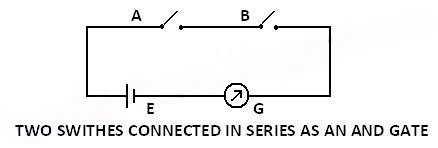
A two-input AND gate can thus be represented by a circuit where two switches are connected in series. Similar principles can be applied to understand the logical functioning of a three-input AND gate.
AND Gate Truth Table
An AND gate, represented in the block diagram, operates with two input signals labelled A and B, producing a single output denoted as Y, where Y equals the logical conjunction of A and B, expressed as Y = AB.
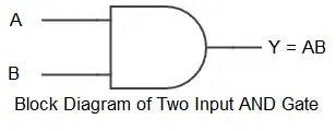
With two input lines, the AND gate accommodates four possible input combinations: 00, 01, 10, and 11. Correspondingly, the outputs generated for these input combinations are 0, 0, 0, and 1, respectively. This behaviour is succinctly captured in a truth table, illustrating the relationship between input and output states for an AND gate with two inputs.
| A | B | Y |
| 0 | 0 | 0 |
| 0 | 1 | 0 |
| 1 | 0 | 0 |
| 1 | 1 | 1 |
The output equation Y = AB signifies the logical operation performed by the AND gate, where the output Y is dependent on both inputs A and B being active simultaneously.
A three-input AND gate combines three input signals, typically labelled A, B, and C, to produce a single output signal, denoted as Y. The output equation for a three-input AND gate is Y = ABC, indicating that the output Y is active (high) only when all three inputs A, B, and C are active (high) simultaneously.
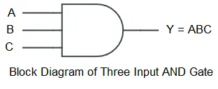
A truth table, also known as a state table, accompanies the AND gate’s block diagram. It lists all possible combinations of input states (000, 001, 010, 011, 100, 101, 110, 111) and their corresponding output states (0, 0, 0, 0, 0, 0, 0, 1).
| A | B | C | Y |
| 0 | 0 | 0 | 0 |
| 0 | 0 | 1 | 0 |
| 0 | 1 | 0 | 0 |
| 0 | 1 | 1 | 0 |
| 1 | 0 | 0 | 0 |
| 1 | 0 | 1 | 0 |
| 1 | 1 | 0 | 0 |
| 1 | 1 | 1 | 1 |
Each row in the truth table demonstrates the behaviour of the AND gate for a specific input combination, showing that the output is only 1 when all inputs are 1, and 0 otherwise. This succinctly summarizes the functioning of the three-input AND gate.
The output equation for an n-input AND gate is expressed as Y = X1 · X2 · X3 · … · Xn, where Y represents the output signal and X1, X2, X3, up to Xn denote the individual input signals.
In this equation, each input, from X1 to Xn, is logically combined using the AND operation. The output Y is active (high) only when all inputs X1 through Xn are active (high) simultaneously. This equation encapsulates the behaviour of an n-input AND gate, illustrating its functionality in digital logic circuits.
AND Gate Using Diodes
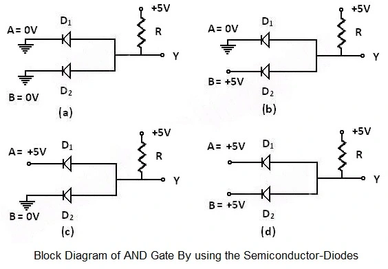
An AND gate can be built using two p-n junction diodes. The Circuit Diagrams of a two-input AND Gate using two p-n junction diodes at four different input stages are shown below.
To construct a two-input AND gate, the positive terminals of the p-n junction diodes are interconnected, forming a junction that functions as the output of the gate. The negative terminals of the diodes serve as the inputs to the gate, representing the two distinct input signals.
Additionally, a resistance R and a +5V voltage source are connected in series with the output to complete the circuit. This arrangement allows the AND gate to perform logical conjunction operations on the input signals, producing the desired output according to the truth table for an AND gate.
In the context of the two inputs A and B and the output Y, a potential of 5V at input A signifies the logical value A = 1, while a potential of 0V at input A represents the logical value A = 0. The same principle applies to input B and output Y. This voltage interpretation aligns with the logical states of the inputs and output of the circuit, allowing for the representation and manipulation of binary logic within the system.
Case One: When A = 0V and B = 0V
When the input terminals A and B of diodes D1 and D2 are grounded, their potentials become 0V, causing the diodes to be forward-biased and offer negligible resistance. Consequently, the potentials at A and B are effectively 0V. Therefore, the potential at point Y equals either A or B. Thus, Y = 0V. The circuit diagram for this case is shown in Figure (a).
Case Two: When A = 0V and B = +5V
When the input A of diode D1 is grounded and input B is at +5V, diode D= becomes forward-biased. Consequently, the potential at Y equals the potential at A. Thus, Y = 0V. The circuit diagram for this case is depicted in Figure (b).
Case Three: When A = +5V and B = 0V
When the first input A is at +5V and the second input B is grounded, the potential at B becomes 0V. Since diode D2 is forward-biased in this configuration, it offers negligible resistance. Consequently, the potential at Y is equal to the potential at B, which is 0V. Therefore, Y = 0V. Figure (c) illustrates the circuit diagram for this scenario.
Case Four: When A = +5V and B = +5V
When the inputs A and B of diodes D1 and D2 are at the same potential of +5V, neither of the diodes conducts any current. If either of the diodes were to conduct any current, a current would flow through resistance R, causing the potential at Y to decrease below 5V, resulting in the diode becoming reverse-biased. Since neither diode conducts any current in this scenario, the potential at Y remains at 5V. Therefore, Y = 5V. Figure (d) displays the circuit diagram for this configuration.
AND Gate using NAND Gate
To implement an AND gate using NAND gates, two NAND gates are employed. The first NAND gate generates the inverted AND gate result. The output of this first NAND gate serves as the input to the second NAND gate, which acts as a single-input NAND gate.
Since a NAND gate with a single input behaves as an inverter, the output of the second NAND gate is the inverted result of the inverted AND gate, which is essentially the output of an AND gate.

The following truth table illustrates the combined NAND gates’ behaviour. This setup effectively implements the AND operation using NAND gates.
| A | B | X | Y |
| 0 | 0 | 1 | 0 |
| 0 | 1 | 1 | 0 |
| 1 | 0 | 1 | 0 |
| 1 | 1 | 0 | 1 |
AND Gate using NOR Gate
To implement an AND gate using NOR gates, three NOR gates are used. The first two NOR gates are used as single-input NOR gates to find the complements of the inputs A and B. Now, the outputs A’ and B’ of the first two NOR gates are fed as inputs to the third NOR gates. Finally, the output of the third NOR gate gives the output of an AND gate.
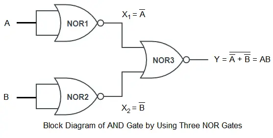
The following truth table illustrates the combined NOR gates’ behaviour. This setup effectively implements the AND operation using NAND gates.
| A | B | X1 = A’ | X2 = B’ | Y = (A’+B’)’ = AB |
| 0 | 0 | 1 | 1 | 0 |
| 0 | 1 | 1 | 0 | 0 |
| 1 | 0 | 0 | 1 | 0 |
| 1 | 1 | 0 | 0 | 1 |
Use of an AND Gate
This gate is fundamental in digital circuitry, often represented by a distinctive logic diagram symbol, and plays a crucial role in various computational and control applications by selectively allowing signal propagation based on input conditions. There are diverse applications of AND gates in various fields of electronics and digital systems.
- Logic Operations: AND gates are fundamental building blocks in digital logic circuits. They’re used to perform logical conjunctions, where the output is true only if all inputs are true.
- Multiplexers and Demultiplexers: In digital electronics, multiplexers and demultiplexers are often constructed using AND gates to select or distribute data among multiple channels.
- Arithmetic Logic Units: ALUs in CPUs use AND gates for various operations such as bitwise AND operations when performing logical operations and for carrying out multiplication operations.
- Flip-flops and Latches: AND gates can be used in the construction of various types of flip-flops and latches, which are essential components in sequential logic circuits used for storing data.
- Address Decoders: In memory systems, address decoders use AND gates to select specific memory locations based on the input address lines.
- Timing Circuits: AND gates can be used in conjunction with other components to create timing circuits that generate specific clock signals or control the timing of signals in digital systems.
- State Machines: State machines and finite state automata often use AND gates to control transitions between states based on input conditions.
- Error Detection and Correction: In error detection and correction circuits, AND gates are used in conjunction with other logic gates to perform parity checks and other error detection algorithms.
- Data Transmission: In communication systems, AND gates can be used to perform bitwise operations on data being transmitted or received to extract specific information.
- Security Systems: AND gates are employed in security systems for implementing logical conditions that must be satisfied before granting access or triggering an alarm.